Demystifying Optical Surface Flatness: Converting λ/20 into Nanometers
On high-precision optical drawings, engineers often encounter a concise yet stringent specification: Surface Flatness λ;/20 @ 632.8 nm. For optical designers and procurement managers, this specification directly dictates component performance, manufacturing yield, and total system cost. Understanding what λ;/20 translates to in absolute physical dimensions—;and how to measure it reliably—;is essential for avoiding costly misunderstandings between optical fabrication shops and quality assurance teams.
01. How Interferometry Measures Surface Topography
Interferometry relies on the principle of optical interference, effectively using the wavelength of light as an ultra-precise physical ruler. A single coherent laser beam is divided into two paths within an optical interferometer:
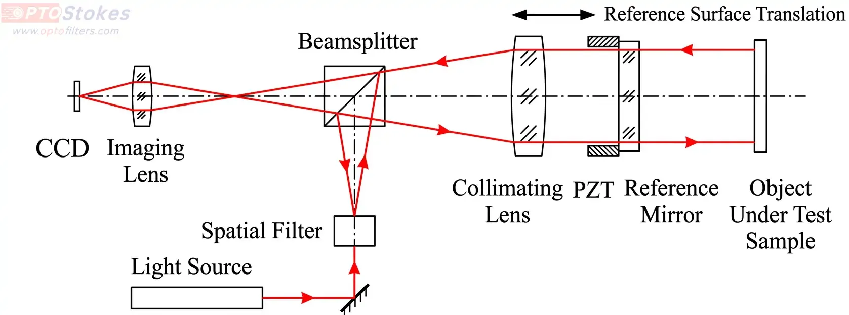
1. Reference Path: Reflected from a known reference surface (a reference flat ground and polished to near-ideal flatness).
2. Test Path: Reflected from the test piece surface (such as an optical flat or mirror).
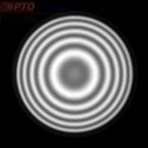
When both reflected beams recombine, constructive interference forms bright fringes (where wave crests align), while destructive interference forms dark fringes (where crests meet troughs). A complete transition from a bright fringe to a dark fringe represents a phase shift caused by a optical path variation.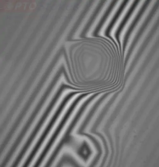
Because light travels to the test surface and reflects back (a two-pass system), a surface height deviation of half a wavelength (λ;/2) introduces a total optical path difference (OPD) of one full wavelength (λ;). Consequently, the spacing between two adjacent interference fringes corresponds to a physical height contour interval of λ;/2. When using a standard Helium-Neon (He-Ne) laser operating at λ; = 632.8 nm, each fringe interval equals approximately 316.4 nm.
Local surface defects—;such as scratches, digs, or localized depressions—;cause straight interference fringes to bend. An optical technician reading fringes is interpreting a topographical contour map: a fringe deviation equal to half the spacing between fringes represents a surface figure error of λ;/4 (~158 nm).
02. Quantifying λ;/20: Converting Wavefront Fractions to Absolute Dimensions
When specifying optical components like Precision Optical Flats & Laser Windows or Custom Optical Mirrors, surface accuracy is defined by two primary metrics:
Peak-to-Valley (PV): The absolute maximum height difference between the highest peak and lowest valley within the clear aperture ($PV = Z_{max} - Z_{min}$).
Root Mean Square (RMS): The statistical standard deviation of surface height variations across the entire measured surface, capturing overall surface quality.
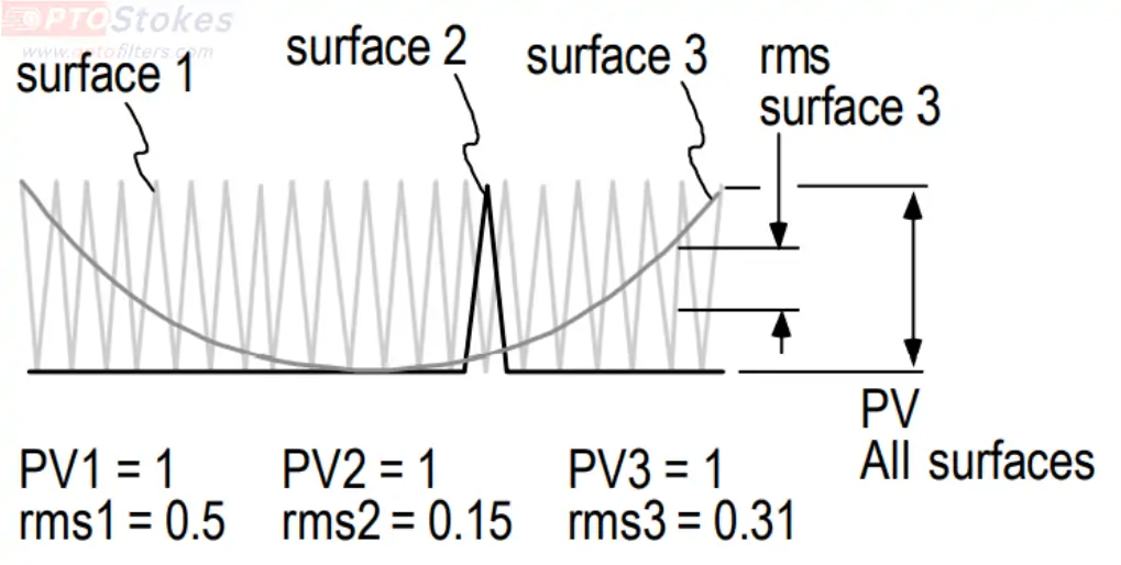
Surface Flatness Scale in Absolute Metrics (He-Ne Laser @ 632.8 nm)
| Specification | Peak-to-Valley (PV) Surface Flatness | Equivalent Dimension in Nanometers | Typical Industrial Applications |
|---|---|---|---|
| λ;/4 | 0.250 λ; | ~158.2 nm | Commercial windows, baseline visual inspection optics. |
| λ;/10 | 0.100 λ; | ~63.3 nm | Precision prisms, high-quality laser line mirrors. |
| λ;/20 | 0.050 λ; | ~31.6 nm | Reference flats, ring laser gyro cavities, ultra-low loss optics. |
A tolerance of λ;/20 represents a physical variation of only 31.6 nanometers. Considering a human hair averages 60 microns (60,000 nm) in diameter, λ;/20 surface error corresponds to roughly 1/1900th of a single hair width.
Critical Pitfall: Surface Figure Error vs. Wavefront Error (WFE)
A frequent point of friction during component acceptance is confounding Surface Figure Error ($\text{PV}_s$) with Wavefront Error ($\text{PV}_w$). In reflective optics operated at normal incidence:
Wavefront Error (PVw) = 2 ×; Surface Figure Error (PVs)
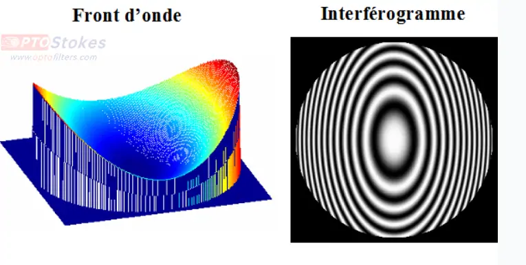
If an optical flat drawing specifies a surface figure of λ;/20 ($\text{PV}_s$), an interferometer reading the reflected wavefront will report a wavefront error of λ;/10 ($\text{PV}_w$). Clarifying whether drawing specifications denote surface figure or reflected wavefront prevents mismatched acceptance criteria.
Furthermore, testing a component to λ;/20 accuracy requires a reference optical flat calibrated to at least 3×; to 5×; higher precision (e.g., λ;/50 to λ;/100 Master Flats), reflecting the rigorous metrology needed to guarantee high-grade optics.
03. Selecting Interferometer Configurations: Fizeau, Twyman-Green, and PDI
Selecting the right metrology method depends on production volume, component geometry, and mechanical stability requirements.
| Interferometer Type | Core Mechanism | Primary Strengths | Limitations & Key Use Cases |
|---|---|---|---|
| Fizeau Interferometer | Common-path design where the reference surface is positioned close to the test piece at the end of the optical path. | Exceptional vibration resistance, minimal air turbulence susceptibility, suitable for 24/7 shop-floor measurement. | Mainstay for production testing of flats, laser windows, and coated optics (e.g., ZYGO, 4D Systems). |
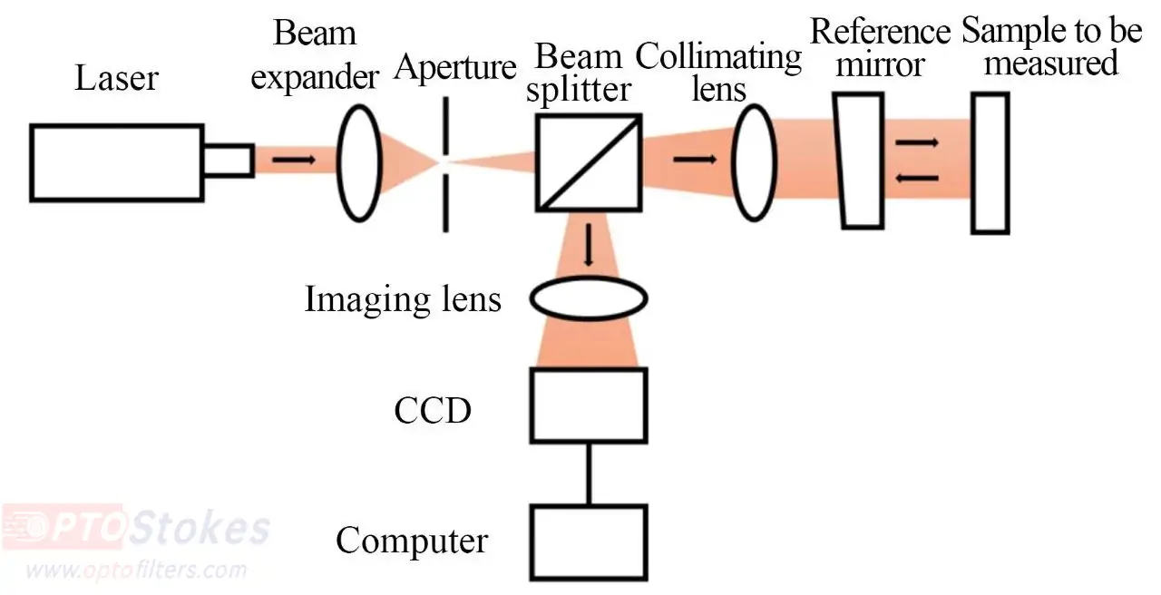
| Twyman-Green Interferometer | Dual-path setup utilizing a beam splitter to divide reference and test arms; derivative of the Michelson interferometer. | Highly versatile for testing complex optics, lenses, prisms, and assembled lens systems. | Separated optical paths make it vulnerable to vibration and air currents; requires optical isolation tables. |
| Point Diffraction (PDI) | Generates a reference spherical wavefront by passing a focused beam through a pinhole of wavelength-scale diameter. | Eliminates physical reference optics; common-path configuration offers high intrinsic stability. | Low light efficiency and complex pinhole alignment. Essential for large-aperture telescope mirrors or EUV lithography optics. |
04. Engineering Support and Precision Optical Solutions by OPTOStokes
Achieving precise surface flatness requires strict control over substrate selection, polishing dynamics, thermal stability, and thin-film coating stress. When sourcing precision optical flats, engineering teams frequently navigate trade-offs between tight fabrication tolerances, lead times, and unit cost.
At OPTOStokes, we specialize in high-precision optical components engineered to meet stringent wavefront and surface quality metrics. Our manufacturing capabilities include:
•; Extensive In-Stock & Custom Inventory: Access a broad range of standard and custom optical flats, windows, and substrates ready for rapid deployment.
•; Verified Quality Control: Every optical flat is validated using advanced Fizeau interferometry, with full surface topography and PV/RMS metrology documentation available.
•; Tailored Fabrication: Custom dimensions, special optical glass substrates (Fused Silica, BK7, Sapphire), and high-damage-threshold coatings tailored to your specific application requirements.
Need technical consultation or custom specifications for your next project? Contact our engineering team at sales@optofilters.com or explore our technical product directory via our optical tags index.