
Product Description
5000nm mid infrared bandpass filter: 240nm bandwidth, 200-11000nm blocking, wide temperature range
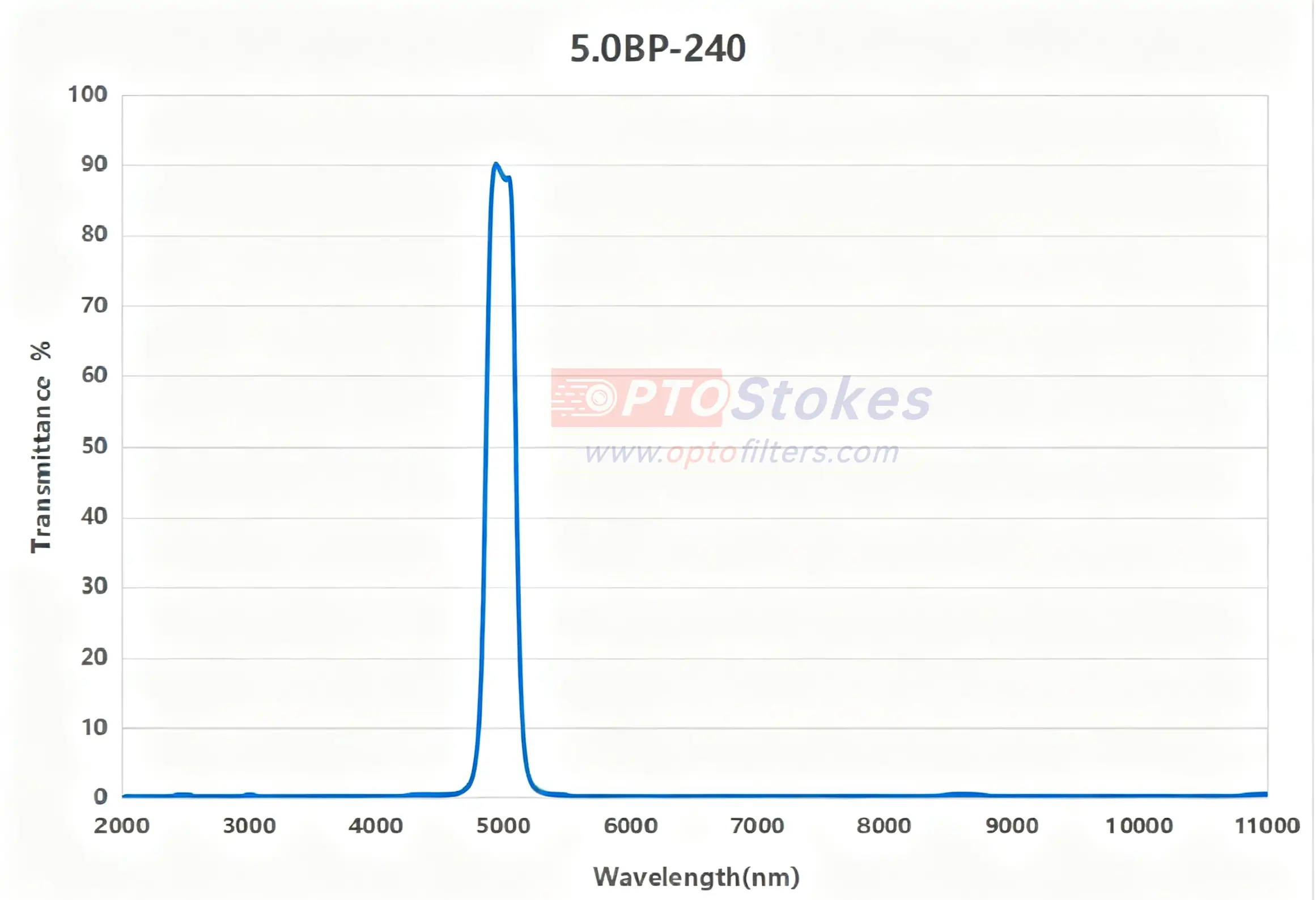
This is a mid infrared bandpass filter with a center wavelength of 5000nm (5.0 μ m) and a full width at half maximum of 240nm, installed in the optical path of gas detection and industrial process control. It is not only worth looking at the spectral parameters separately, but also the temperature range: high and low temperature tests were conducted at -45 ℃ and 125 ℃ according to IEC 60068-2-1 and IEC 60068-2-2 respectively - this span determines whether it can be installed in field equipment or can only be used on laboratory prototypes.
Technical specifications
| Parameters | Specifications | Description |
|---|---|---|
| Product Model | IR Bandpass Filter 5000nm | The wavelength and bandwidth are as follows |
| Center wavelength CWL | 5000 ± 40nm (5. 0um ± 0.04 μ m) | Transmittance at this wavelength T>; 80% |
| FWHM | 240 ± 30nm (0.24 ± 0.03 μ m) | Transmittance drops to 50% of the peak, with a distance between two points |
| Transmittance | T>at 5000nm; 80% | Single point indicator, the lowest passband value is based on the measured curve |
| Blocking range | 200-11000nm (excluding passband), OD> 2 | OD2 corresponds to a transmittance of 1% |
| Base material | Silicon wafer/sapphire | The two materials exhibit different behavior at 5.0 μ m, confirmed by model |
| Low temperature test | IEC 60068-2-1/GB/T 2423.1, Test A, -45 ℃ | The specific number of cycles and criteria shall be in accordance with the test report |
| High temperature test | IEC 60068-2-2/GB/T 2423.2, Test B, 125 ℃ | The specific number of cycles and criteria shall be in accordance with the test report |
| Incident angle/thickness/size | Confirm according to inquiry | No fixed specifications specified on this page |
Let me explain two points first. The blocking interval is written as "passband excluded": 5000nm falls within the range of 200-11000nm, and the blocking commitment refers to the entire segment outside the passband. The value of 80% transmittance is lower than the common level in the visible wavelength band, and the reason is not due to conservative design - the available high refractive index coating materials for mid infrared are already limited, and the substrate also absorbs near this wavelength. With too many film layers, the loss cannot be suppressed. Seeing 80%, there is no need to rush to find higher alternatives. First, confirm the testing conditions and substrate materials.
Silicon wafer or sapphire: these two options are not equivalent
It is easy to mistake the specification for "silicon wafer/sapphire" as an option of the same price. In fact, at the 5 μ m position, the constraints of the two materials are completely different. The conventional transmittance range of optical silicon is 1.2-7 μ m, but there is absorption caused by lattice vibration near 5 μ m, and the actual transmittance is significantly lower than its level of 1.5-3 μ m; The upper limit of sapphire transmission is around 5.0 μ m, and although 5 μ m is available, it is already close to the long wave boundary, and the passband will fall quickly if it moves further towards longer wavelengths.
Another difference lies in reflection. The refractive index of silicon is about 3.4, and the single-sided reflection loss is close to 30%. To achieve 80% transmission, it highly depends on the design of the anti reflection film; Sapphire has a refractive index of about 1.7 and much lower self reflection loss, leaving a larger margin for the film system. So these two options correspond to different cost structures and wavelength margins, not just randomly selected ones. If the center of the passband may be adjusted towards longer wavelengths, the boundaries of sapphire will become restrictions earlier.
NDIR gas detection: a parameter based selection deduction
The following is a deduction example, not a customer case.
Requirement: Infrared gas analysis module for industrial sites or environmental monitoring, equipped with broadband infrared light source and pyroelectric or thermopile detector, capable of measuring target absorption near 5.0 μ m and outputting concentration or alarm signals.
Why 240nm instead of narrower: These systems use broadband light sources, and the bandwidth is too narrow to receive enough energy, resulting in a decrease in signal-to-noise ratio. 240nm is a compromise between "receiving light" and "avoiding adjacent absorption bands"; The specific width depends on the distance between the target gas and the interfering gas in that frequency band.
Why blocking at 200-11000nm is key: thermal detectors are broadband, responding from near-infrared to long wavelength infrared. The filter does not just need to block a certain line, but to compress the entire section that the detector can respond to, otherwise the out of band radiation of the light source and the environmental thermal background will enter. This span covers the response range of the vast majority of thermal detectors, which is also the reason why it can be equipped with multiple detectors.
Why wide temperature testing is not decoration: the working temperature of on-site equipment may range from -45 ℃ to 125 ℃. The thermal expansion coefficients of the film layer and substrate do not match, and temperature cycling can accumulate stress within the film layer, resulting in center wavelength drift, edge deformation, and in extreme cases, film cracking. The difference in thermal expansion coefficient between sapphire and silicon is more than twice, so this one should be considered before the price when selecting materials.
Applicable boundary: The parameters are calibrated at room temperature, and the actual curve at extreme temperatures may deviate; The blocking depth is designed according to OD2 and is suitable for medium sensitivity concentration measurement. Trace detection requires a higher level.
Before placing an order, it is necessary to verify the wavelength retest data before and after temperature cycling, rather than just looking at the conclusion of "passing the test"; The measured blocking curve for the entire range of 200-11000nm, with a focus on the band transition; Is the response range of the detector aligned with the blocking interval.
Two easily trampled misjudgments
One is to regard "passing high and low temperature tests" as "temperature changes do not affect performance". The test proves that failure, detachment, and cracking do not mean that the wavelength has no drift. It is entirely possible for the 240nm passband to drift a few nanometers between -45 ℃ and 125 ℃, but it has limited impact on gas measurements with wide absorption bands. For narrow line measurements, it is enough to cause the signal to drop by half. The correct approach is to compare the center wavelength before and after the cycle with the measured bandwidth, and use the drift as a design margin instead of assuming it to be zero.
The second is to increase OD>; 2 means that every nanometer meets the standard. The span of 200-11000nm exceeds 10000 nanometers, and it is difficult to maintain the entire process with a single film system. In reality, it is mostly segmented plating or multi piece combination, and the junction between segments is often the worst. Acceptance is based on the average value of the samples, and although compliance is observed everywhere, it is possible that there may be only slightly more OD1 in a narrow range. However, the response of the thermal detector is broadband, and the worst part will still be integrated. The contract should specify the minimum value for the entire section and require the provision of continuous scanning curves.
Customization and delivery support
The passband center and bandwidth can be adjusted according to the project, the substrate material can be specified, the anti reflection design can be optimized to improve transmittance, the blocking interval can be expanded, and the shape and card mounting method can be changed. Samples and measured spectral data can be provided by project, and the original records of high and low temperature tests and retest data after cycling can also be requested by project. Batch applications require a batch consistency aperture with a center wavelength of ± 40nm and a bandwidth of ± 30nm. The selection ideas for mid infrared gas detection can refer to<a href=“ https://www.optofilters.com/article/case/LWIR-Filter-Selection-for-NH3-Sensors.html Selection case of mid infrared gas detection filter; for more infrared bandpass specifications, please refer to<a ref=" https://www.optofilters.com/product/OpticalFilters.html Classification of Optical Filter Products
Information required for inquiry
Please provide: target center wavelength and bandwidth, absorption positions of target gas and interference gas, light source type and detector model, optical path length, operating temperature range, substrate material inclination (silicon or sapphire), external dimensions and aperture, annual usage. The fifth and sixth items are most often missed, but they directly determine whether this area can survive on site. Technical Consultation and Inquiry: sales@optofilters.com , or through<a ref=“ https://www.optofilters.com/single/contact-us.html Contact us on thepage to submit.
Tags: 5000nm infrared filter mid infrared bandpass filter 5.0 μ m filter gas detection filter silicon substrate filter sapphire filter