
Product Description
BP2.3um mid infrared bandpass filter: 2.3 μ m center wavelength, 120nm bandwidth, 0.4-11 μ m blocking
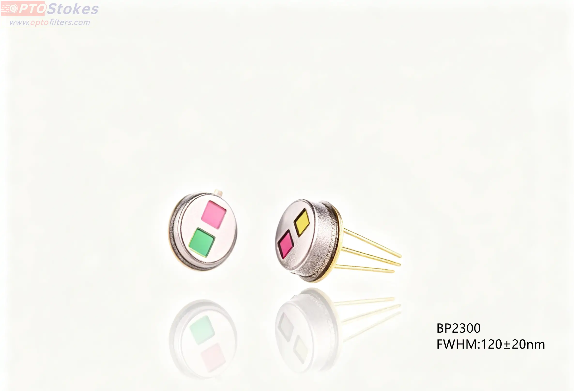
BP2.3um is a bandpass filter with a center wavelength of 2.3 μ m (2300nm) and a full width at half maximum of 120nm. It is installed in front of the detector of a near-infrared spectrometer to select the measurement window near 2.3 μ m and block the radiation of the light source in other bands. The actual constraint of this band is not in the membrane design, but in the material: there are only a few substrates that can penetrate 2.3 μ m and remain stable for a long time. If the material is chosen incorrectly, the transmittance curve will first collapse outside the drawing.
Technical specifications
| Parameters | Specifications | Description |
|---|---|---|
| Product model | BP2.3um | The wavelength and bandwidth are subject to the following table |
| Center wavelength CWL | 2.3 μ m (2300nm) | Transmittance at this wavelength T>; 85% |
| FWHM | 120 ± 20nm (0.12 ± 0.02 μ m) | Transmittance drops to 50% of the peak, with a distance between two points |
| Transmittance | T>at 2.3 μ m; 85% | Single point indicator, the lowest passband value is based on the measured curve |
| Blocking range | 0.4-11 μ m (excluding passband), OD> 2 | OD2 corresponds to a transmittance of 1% |
| Substrate material | Confirm according to inquiry | 2.3 μ m available materials are limited, directly determining the price and long wave blocking |
| Incident angle | Not specified, quoted and tested at 0 ° | Convergent or oblique incident optical paths must be separately specified |
| Thickness/Shape | Confirm according to inquiry | No fixed specifications specified on this page |
First, unify the unit. 2.3 μ m is 2300nm, and 120nm bandwidth is 0.12 μ m, both of which are two ways of writing the same thing. The original specifications use micrometers for the center wavelength and nanometers for the bandwidth, which can easily cause misalignment when read; When writing a purchase order, fixing the unit can avoid ordering at 2400nm or 2600nm. This wavelength is stuck at the long wavelength end of near-infrared, and the next step towards long wavelength is mid infrared. Different companies have different definitions of the wavelength boundary for "near-infrared spectrometers", so it is safest to directly provide numerical values during communication.
The second thing to note is that T>; 85%. This value is lower than the common level in the visible band, not because of conservative design, but because of material limitations: there are few types of high refractive index coating materials available for mid infrared, and the substrate itself has weak absorption near 2.3 μ m. As the number of film layers increases, the accumulation of absorption and scattering consumes a few percentage points. Don't rush to find a 90% replacement when you see 85%, you need to confirm the testing conditions and substrate of the other party first.
Near infrared spectrometer: a parameter based selection deduction
The following is a deduction example, not a customer case.
Requirement: Near infrared analyzer with filter wheel or fixed channel, halogen lamp as light source, measuring C-H and O-H combined frequency absorption near 2.3 μ m for rapid determination of moisture and organic matter content, detector for extended InGaAs or PbS..
Why 120nm: The absorption band in this band is relatively wide, and if the bandwidth reaches 20nm, it will not receive enough photons, resulting in a decrease in signal-to-noise ratio.. 120nm is a compromise of "separating and receiving light", belonging to the concept of broadband bandpass filters, not narrowband filters.
Why does OD2 depend on the light source?Here, we can't just look at the numbers.. Halogen lamps are broad-spectrum blackbodies that still have a large amount of energy beyond 2.3 μ m, especially at the short wave end; OD2 compresses this part to 1%, whether it is enough depends on how much stronger the out of band light is than the signal, rather than whether the number 1% looks good or not.
Applicable boundary: The upper limit of detector response is within 11 μ m; The spectrum of the light source should not be too strong; The optical path is collimated, and the filter receives light almost vertically.
Before placing an order, it is necessary to verify the substrate material and its permeability at 2.3-3 μ m; The measured transmission curve of the entire 2.0-2.6 μ m band, rather than the center point; The integral value obtained by multiplying the out of band leakage with the light source spectrum and detector response.
Two easily trampled misjudgments
One is to use the experience of visible wavelength bands to select substrates for 2.3 μ m. Ordinary BK7 has obvious absorption at this wavelength, and fused quartz has also begun to be affected by the hydroxyl absorption band around 2.3 μ m, both of which are not materials that can be used as expected. The consequence of choosing the wrong one is not "lower transmittance", but rather the whole piece does not meet the standard, the curve shape deforms, and in severe cases, the film layer fails after temperature and humidity cycling. 2.3 μ m commonly used calcium fluoride, sapphire, or infrared grade quartz. The specific choice depends on whether to achieve 11 μ m blocking and cost constraints. When inquiring, it is much more useful to include the working band and existing detectors together, rather than just reporting one central wavelength.
Secondly, OD>; Write OD as' sufficient '. OD2 has a transmittance of 1%, and the number itself is harmless, but the interference caused by light leakage depends on how strong the out of band light is. The radiation intensity of a blackbody light source near 1 μ m is much higher than that of 2.3 μ m. If that segment is two orders of magnitude stronger than the signal, 1% of the leaked light is of the same magnitude as the signal. The correct approach is to multiply the spectrum of the light source, the measured blocking curve, and the detector response, and integrate them to determine the proportion of the total amount that leaks into the detector in the signal; Only checking the OD value is equivalent to compressing three variables into one to determine.
Customization and delivery support
The shape can be adjusted according to the project (circular, square, irregular), equipped with a set of card rings, and the substrate and coating design can be changed, including extending the blocking interval beyond 11 μ m, improving the OD level, and redesigning according to the actual working angle. The substrate is the variable that needs to be locked in advance in this specification, and it should be determined during the sample stage to avoid curve rework due to material switching during mass production. Samples and measured spectral data can be provided by project. The channel configuration idea of filter based near-infrared spectrometer can refer to<a ref=“ https://www.optofilters.com/article/case/271.html Application case of filter type near-infrared spectrometer; see<a ref=for complete category https://www.optofilters.com/product/OpticalFilters.html Classification of Optical Filter Products
Information required for inquiry
Please provide: working center wavelength and bandwidth, light source type and color temperature, detector model and response range, specific wavelength band and OD for blocking requirements, external dimensions and aperture, annual usage, and whether a moisture resistant substrate is needed. The second and third decisions determine whether the OD is sufficient, while the fourth and seventh decisions determine how to choose the substrate. Technical Consultation and Inquiry: sales@optofilters.com , or through<a ref=“ https://www.optofilters.com/single/contact-us.html Contact us on thepage to submit.
Tags: SWIR filter 2.3 μ m bandpass filter 2300nm bandpass filter mid infrared filter near-infrared spectrometer filter BP2.3um