
Products Description
BP975nm bandpass filter: 975nm ± 3nm, 25nm bandwidth, 350-1100nm blocking
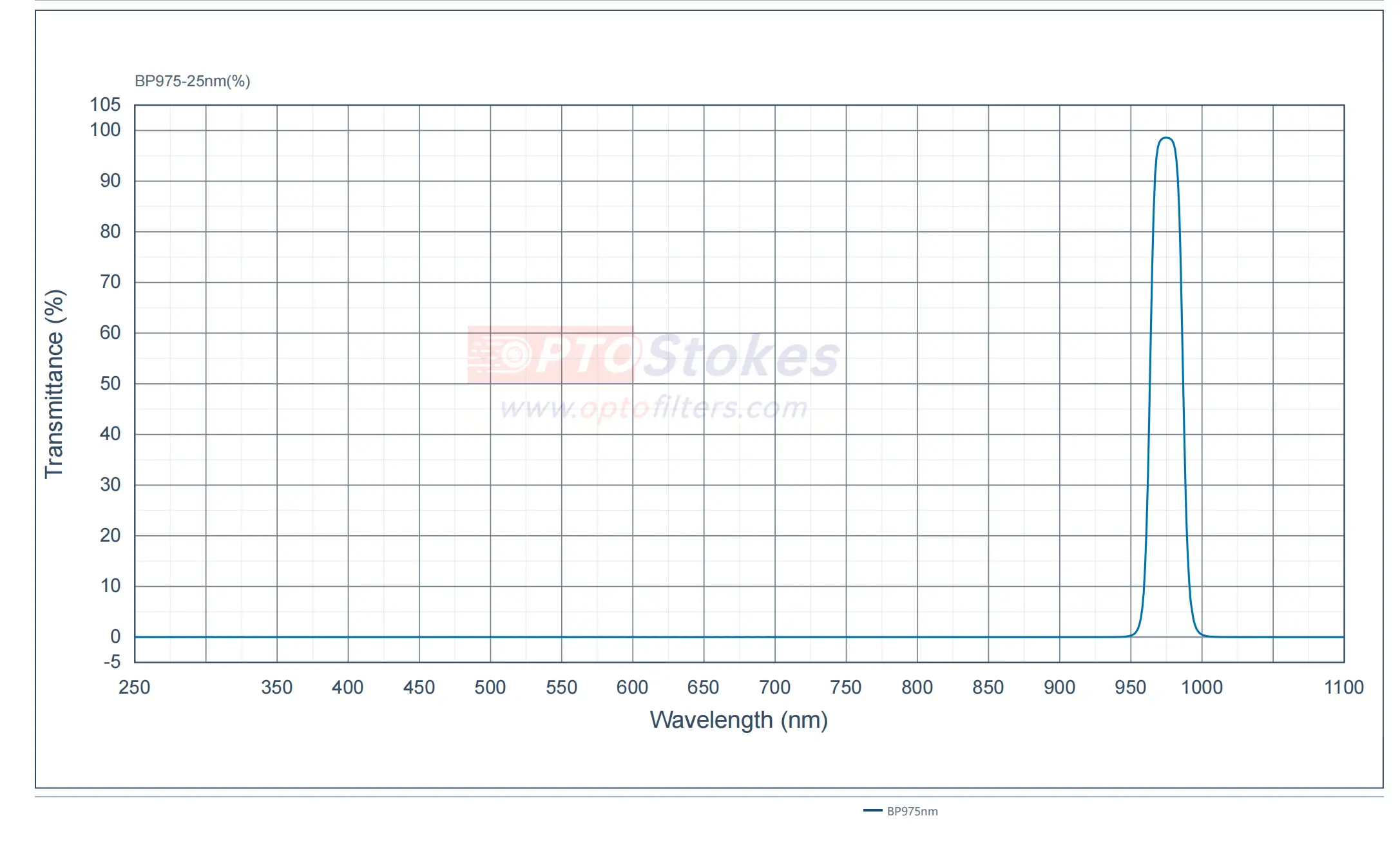
BP975nm is a near-infrared bandpass filter with a center wavelength of 975nm and a half width of 25nm, used in auxiliary optical channels for short-range infrared sensing and industrial temperature measurement. Its blocking range of 350-1100nm almost overlaps with the response range of silicon detectors, which means that every wavelength that silicon can respond to is blocked outside, only the 25nm passband comes in - compared to simply looking at OD values, this range line can better indicate its positioning.
Technical specifications
| Parameters | Specifications | Description |
|---|---|---|
| Product model | BP975nm | The wavelength and bandwidth are subject to the following table |
| Center wavelength CWL | 975 ± 3nm | Transmittance at this wavelength T>; 90% |
| FWHM | 25 ± 3nm | When the transmittance drops to 50% of the peak, the distance between two points |
| High transparency band | 970-985nm, T>; 90% | High transmittance interval within the passband, with edge shape based on the measured curve |
| Blocking range | 350-1100nm (excluding passband), OD> 2 | OD2 corresponds to a transmittance of 1% |
| Incident angle | Not specified, quoted and tested at 0 ° | When equipped with diverging light sources such as LED, separate instructions must be provided |
| Thickness/Shape/Substrate | Confirm according to inquiry | No fixed specifications specified on this page |
There is one thing that needs to be clarified in advance. The high transmittance region between 970-985nm has a width of 20nm and a full width at half maximum of only 25nm, indicating a relatively high ratio between the two. This suggests that the edge of this curve is quite steep - the drop from 90% to 50% may only occur within a few nanometers. This design can be achieved, but it requires high control over the film layer. The actual shape and edge landing point should be based on the manufacturer's measured curve, rather than being calculated based on an ideal rectangle. Especially at the 975nm end, which is already very close to the halfway point, if the wavelength of the light source is precisely pressed at this position, the actual transmittance cannot be estimated at 90%. Similarly, the blocking range is written as "passband excluded": 975nm itself falls within 350-1100nm, and the blocking commitment refers to the part outside the passband.
Industrial temperature measurement auxiliary channel: a parameter based selection deduction
The following is a deduction example, not a customer case.
Requirement: Add an auxiliary optical channel to the infrared thermometer, using LED or small light sources for illumination and reference, and a silicon detector for reception. It is necessary to suppress the lighting in the factory, the hot background near the measured object, and the leakage of sunlight.
Why 25nm instead of 5nm: The signal from short-range sensing is strong enough, and there is no need to rely on extremely narrow bandwidth for selectivity; Relaxing the bandwidth to 25nm can capture more light while reducing the risk of wavelength drift in the light source. Narrowband chips are over designed here, at the cost of cost and alignment difficulty.
Why is the 975nm position suitable? It is close to the long wave end of the silicon detector response, and the response is still available; At the same time, it avoids the water vapor absorption band near 940nm and is more stable than 940nm in situations with a certain optical path length.
Why OD2 is sufficient: short distance, strong signal, and 1% light leakage account for a very low proportion of the total amount. If it is replaced with outdoor strong sunlight, long optical path, or when the measured temperature is close to the ambient temperature, the proportion of light leakage will increase. In this case, it is necessary to increase the blocking level instead of compensating in the software.
Applicable boundary: silicon detector; The optical path length is within meters; The ambient temperature is not higher than the conventional industrial environment; The light source has basic collimation.
Before placing an order, it is necessary to verify the alignment between the actual peak wavelength of the light source and the passband; Residual divergence angle of LED after collimation; The measured transmittance at 970nm and 985nm ends, rather than just looking at the center point.
Two easily trampled misjudgments
One is to use a 975nm light source to match this piece. The difference between 970nm and 985nm is only 15nm, which looks not far, but the passband is only 25nm. This type of combination may barely be counted in the laboratory. If you change a batch of chips or a batch of light sources, the signal will drop off - the problem is not the quality of the film system, but the insufficient parameter margin itself. When selecting, overlay the peak wavelength of the light source and the passband curve on the same graph for comparison, rather than just focusing on the center wavelength; If the peak of the light source is pressed on the shoulder, changing to a specification with a center wavelength closer to it is much more convenient than compensating in the system.
The second is to ignore the divergence angle of the light source. Short distance infrared sensors commonly use LEDs, which have divergence angles of several tens of degrees and residual angles even after simple collimation. The passband of a bandpass filter shifts towards shorter wavelengths as the incident angle increases. The 25nm passband may drift off by a few nanometers when obliquely incident at more than ten degrees, resulting in a decrease in effective transmission of the edge field of view. This phenomenon is characterized by a bright center, dark edges, or signal loss as the distance changes. When using LED as a light source, do not estimate performance based on a 0 ° curve: either make the collimation solid, or write the actual working angle into the inquiry conditions and let the manufacturer design according to the angle.
Customization and delivery support
The shape can be adjusted according to the project (circular, square, irregular), matched with a set of card rings, and the substrate and coating design can be changed, including adjusting the center wavelength to align with the peak value of a specific light source, redesigning according to the actual working angle, increasing the blocking level, and extending the blocking range beyond 1100nm. Samples and measured spectral data can be provided by project. Batch applications require prior agreement on batch consistency with a center wavelength of ± 3nm - when multiple devices share a set of calibration parameters, the wavelength distribution directly determines whether calibration is required for each device. For the complete category, please refer to<a ref=“ https://www.optofilters.com/product/OpticalFilters.html Classification of Optical Filter Products
Information required for inquiry
Please provide: light source type and actual peak wavelength, detector response range, working incident angle or light source divergence angle, optical path length, external dimensions and aperture, annual usage, and working temperature range. The first and third ones are most often missed, but they directly determine whether this piece can be used - the peak wavelength determines which section of the passband it falls on, and the divergence angle determines whether the actual curve will shift. Technical Consultation and Inquiry: sales@optofilters.com , or through<a ref=“ https://www.optofilters.com/single/contact-us.html Contact us on thepage to submit.
Tags: NIR bandpass filter 975nm narrowband filter 975nm bandpass filter infrared temperature measurement filter silicon detector filter BP975nm